

Cleanroom Device Fabrication Experience:
Cleanroom Environment:
- Proficient in working in a 1000* class cleanroom environment.
- Specialized in both optical and e-beam lithography.
Optical Lithography:
- Extensive use of tools such as mask aligner and laser writer.
- Competent in handling both positive and negative photoresist.
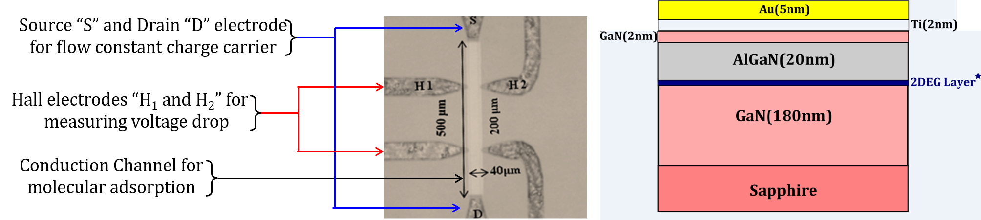
GaN/AlGaN 2D Electron Gas Hall Device Fabrication:
- Expertise in the fabrication of GaN/AlGaN 2D electron gas hall devices.
- Involved in chip designing using a comprehensive set of instruments.

Instrument Proficiency:
- Adept in the cleanroom bench photoresist coating process.
- Skilled in laser, e-beam, and optical mask alignment.
- Proficient in the development process.
- Experienced in oxygen and argon plasma cleaning.
- Competent in e-beam metal deposition and liftoff techniques.
- Capable of rapid thermal treatment.
- Skilled in inductive coupled plasma etching.
- Expertise in SiN isolation through Plasma-Enhanced Chemical Vapor Deposition (PECVD).
- Proficient in pad and channel opening processes.
Sputtering Techniques:
- Experience with RF and DC (AJA) sputtering tools for soft ferromagnetic thin film deposition, particularly for spintronics devices.
Atomic Layer Deposition:
- Proficient in Atomic Layer Deposition techniques for various oxide depositions, specifically for GaAs/AlGaAs and 2DEG spintronics devices.
- Buffer layer for 4-probe magnetoresistance devices.
Atomic Force Microscopy (AFM):
- Utilized AFM for nanoscopic conduction measurements, particularly in the presence of external magnetic fields.
- Expertise in investigating magnetoresistance at the nanoscopic level.